
Crystal Orientation
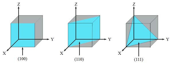
Silicon crystal planes
Silicon has a diamond lattice structure where each atom forms four identical covalent bonds with its neighbours in a tetrahedral arrangement. Within the crystal lattice there are several crystal planes, identified in the diagram on the right using the Miller Indices.
Although silicon ingots are available with the major ingot axis grown in a number of different orientations, it is often necessary to precisely cut the ingot, either to obtain a section with the correct orientation and finished size for the final crystal, or to provide a specific crystal orientation (e.g. a <311> cut).
Crystal Scientific use an X-ray diffraction system to identify the planes in the crystal structure and to check the precise orientation of the crystals for machining to an accuracy of 0.05 degrees. This is achieved using a specially designed bond jig. The orientated material is then precision-transferred to the diamond machining stage.
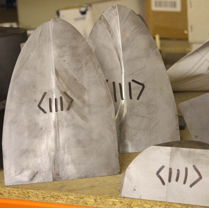
Silicon cut to <111> plane
The completed diffraction optic is characterised using a Bede 200 high-resolution double crystal diffractometer and the final test data showing the rocking curve width is included in the metrology reports for the customer.
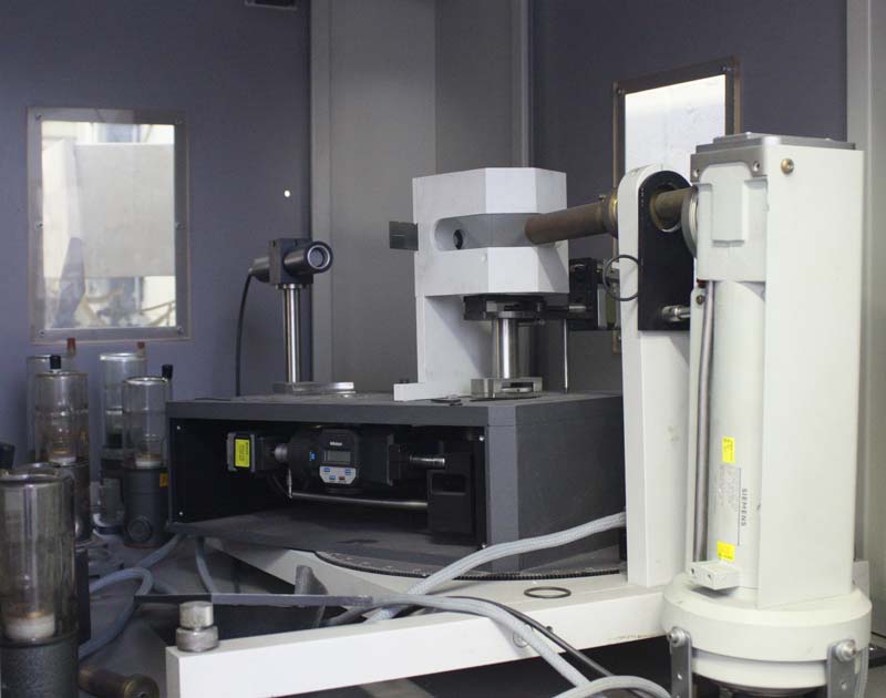
X-ray diffraction machine